 |
 |
| Copper substrate cut into working panel size |
Inner image transfer process
Photoresist (dry film)=>Exposure=>Development=>Etching |
 |
 |
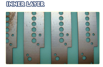
The inner of the copper surface is roughened with
liquid chemicals to increase the prepreg binding force |
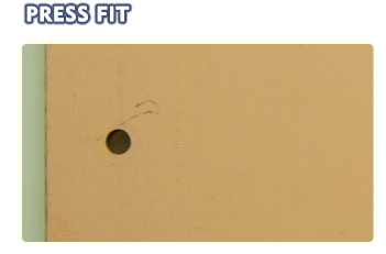
Press fit uses high temperatures to make layers of material
Combine |
 |
 |
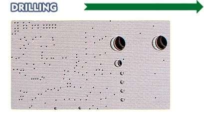
Mechanical drilling uses work files to
drill through layers via positioning |
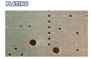
Full board plating with copper to let all apertures do copper conduction process.
Desmear => Chemical copper => Copper plating |
 |
 |
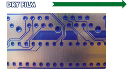
Outer image transfer using film for printing process
Photoresist (dry film) => Exposure => Developer |
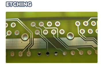
Image that finished etching and transferring,
using copper chloride to
bite the exposed copper,
allowing the blue photoresist to
remain on the surface of the board.
Etching => Removing the film |
 |
 |
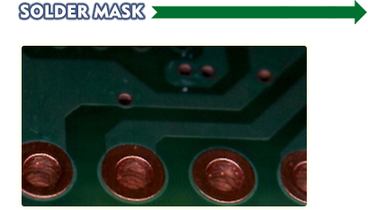
Solder mask printing surface and filling designated via to make its circuit insulation anti-oxidation process
Ink Printing => Exposure => Development => Baking |
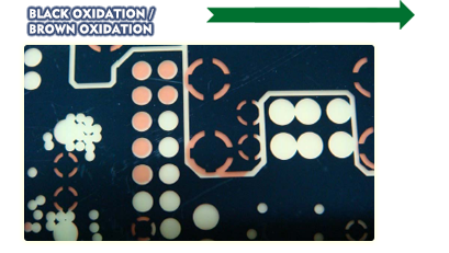
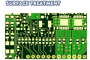
Electroless Nickel/Immersion Gold(ENIG) treatment uses
the principle
of dip-plating and transposition so that it does
not cover the area
of the bare copper surface
to form a metal cladding.
Process dip palladium => nickel dip => dipping gold |
 |
 |
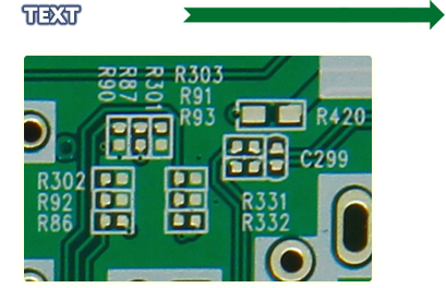
| Text using ink printed font |
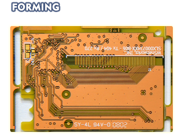
CNC type mechanical forming frame and inner tank, using V-cut on the panelization. |
 |
 |
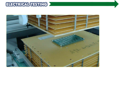
Circuit Test Confirms Functionality of Wire and VIA
(100% test) |
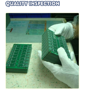
Visual inspection confirms that the material is in compliance
with the standard specification
(100% inspection) |